

Understanding Your Graphics Card: A Look Inside Your GPU


How many calculations do you think your graphics card performs every second while running video games with incredibly realistic graphics? Maybe 100 million? Well, 100 million calculations a second is what’s required to run Mario 64 from 1996. To run the most realistic video games such as Cyberpunk 2077 you need a graphics card that ca perform around 36 trillion calculations a second.
Imagine doing a long multiplication problem once every second. Now let’s say everyone on the planet does a similar type of calculation but with different numbers. To reach the equivalent computational power of this graphics card and its 36 trillion calculations a second we would need about 4,400 earths filled with people, all working together and completing one calculation every second.
In this blog, we’ll explore the different components inside a graphics card, as well as the physical design and architecture of the GPU. We’ll also explore the computational architecture and see how GPUs process mountains of data, and why they’re ideal for running video game graphics, bitcoin mining, and AI.
GPU vs CPU
Inside a graphics card, the Graphics Processing Unit or GPU has over 10K cores. However, when we look at the Central Processing Unit or CPU that’s mounted to the motherboard, we find an integrated circuit or chip with only 24 cores. So, which one is more powerful? 10K is a lot more than 24, so you would think the GPU is more powerful, however, it’s more complicated than that.
A useful analogy is to think of a GPU as a massive cargo ship and a CPU as a jumbo jet airplane. The amount of cargo capacity is the amount of calculations and data that can be processed, and the speed of the ship or airplane is the rate at which how quickly those calculations and data are being processed. Essentially, it is a trade-off between a massive number of calculations that are executed at a slower rate versus a few calculations that can be performed at a much faster rate. Airplanes are a lot more flexible since they can carry passengers, packages, or containers and can take off and land at any one of tens of thousands of airports. Likewise CPUs are flexible in that they can run a variety of programs and instructions. However, giant cargo ships carry only containers with bulk contents inside and are limited to traveling between ports. Similarly, GPUs are a lot less flexible than CPUs and can only run simple instructions like basic arithmetic. Additionally, GPUs can’t run operating systems or interface with input devices or networks.
If you want to perform a set of calculations across mountains of data, then a GPU will be faster at completing a task. However, if you have a lot less data that needs to be evaluated quickly then a CPU will be faster. Furthermore, if you need to run an OS or support network connections and a wide range of different applications and hardware, then you will want a CPU.
Inside a Graphics Card
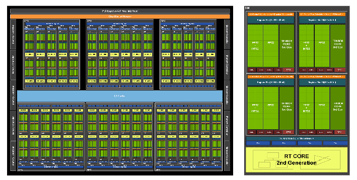
In the center of a graphics card is the printed circuit board or PCB, with all the various components mounted on it. The brains of the operation is the GPU. When opened up, we find a large chip or die named GA102 build from 28.3 billion transistors. The majority of the area of the chip is taken up by the processing cores which have a hierarchical organization. The chip is divided into 7 Graphics Processing Clusters or GPCs, and within each processing cluster are 12 streaming multiprocessors or SMs. Next, inside each of these streaming multiprocessors are 4 warps and 1 ray tracing core, and then inside each warp are 32 CUDA or shading cores and 1 tensor core. Across the entire GPU, there are 10752 CUDA cores, 336 tensor cores, and 84 ray tracing cores. these three types of cores execute all the calculations of the GPU, and each has a different function. CUDA cores can be though of as simple binary calculators with an addition button, a multiply button and a few others, and are used the most when running video games. Tensor cores are matrix multiplication and addition calculators and are used for geometric transformations and working with neural networks and AI. Ray tracing cores are the largest but the fewest and are used to execute ray tracing algorithms.
Interestingly, the 3080, 3090, 3080 ti, and 3090 ti graphics cars all use the same GA102 chip design for their GPU. During the manufacturing process sometimes patterning errors, dust particles, or other manufacturing issues cause damage and create defective areas of the circuit. Instead of throwing out the entire chip because of the small defect, engineers find the defective region and permanently isolate and deactivate the nearby circuitry. By having a GPU with highly repetitive design, a small defect in one core only damages that particular SM circuit and doesn’t affect the other areas of the chip. As a result, these chips are tested and categorized or binned according to the number of defects. The 3090ti graphics cards have flawless GA102 chips with all 10752 CUDA cores working properly, the 3090 has 10496 cores working, the 3080ti has 10240 and the 3080 had 8704 CUDA cores working, which is equivalent to having 16 damaged and deactivated SMs. Different graphic cards differ by their maximum clock speed and the quantity of generation of graphics memory that supports the GPU.
Zooming into one of these CUDA cores, inside this simple calculator is a layout of approximately 410 thousand transistors. This section of 50 thousand transistors performs the operation of A times B plus C which is called fused multiply and add or FMA and is the most common operation performed by graphics cards. Half of the CUDA cores execute FMA using 32-bit floating-point numbers, which is essentially scientific notation, and the other half of the cores use either 32-bit integers or 32-bit floating point numbers. Other sections of this core accommodate negative numbers and perform other simple functions like bit-shifting and bit masking as well as collecting and queueing the incoming instructions and operands, and then accumulating and outputting the results. As a result, this single core is just a simple calculator with a limited number of functions. This calculator completes one multiply and one add operation each clock cycle and therefore with a 3090 graphics cards and its 10496 cores and 1.7 gigahertz clock, we get 35.6 trillion calculations a second. These calculator operations are performed by the special function units which are far fewer as only 4 of them can be found in each streaming multiprocessor.
Around the edge of the GA102 chip we find 12 graphics memory controllers, the NVLink Controllers and the PCIe interface. On the bottom is a 6-megabyte Level 2 SRAM Memory Cache, and the Gigathread Engine manages all the graphics processing clusters and streaming multiprocessors inside.
On one side are the various ports for the displays to be plugged into, on the other side is the incoming 12 Volt power connector, and then the PCIe pins that plug into the motherboard. On the PCB, the majority of the smaller components constitute the voltage regulator module which takes the incoming 12 volts and converts it to one point one volts and supplies hundreds of watts of power to the GPU. Because all this power heats up the GPU, most of the weight of the graphics card is in the form of a heat sink with 4 heat pipes that carry heat from the GPU and memory chips to the radiator fins where fans then help to remove the heat.
Aside from the GPU, the 24 gigabytes of graphics memory chips which are technically called GDDR6X SDRAM are some of the most important components. Whenever you start up a video game or wait for a loading screen, the time it takes to load is mostly spent moving all the 3D models of a particular scene or environment from the solid-state drive into these graphics memory chips. The GPU has a small amount of data storage in its 6-megabyte shared Level 2 cache which can hold the equivalent of a small portion of the video game’s environment. Different chunks of scene are continuously being transferred between the graphics memory and the GPU in order to render a video game. Because the cores are constantly performing tens of trillions of calculations a second, GPUs are data hungry machines and need to be continuously fed terabytes upon terabytes of data, and thus these graphics memory chips are designed kind of like multiple cranes loading a cargo ship at the same time. These 24 chips transfer a combined 384 bits at a time, which is called the bus width and the total data that can be transferred, or the bandwidth is about 1.15 terabytes a second. In contrast the sticks of DRAM that support the CPU only have a 64-bit bus width and a maximum bandwidth closer to 64 gigabytes a second.
Computers do not only work using binary ones and zeros. In order to increase data transfer rates, GDDR6X and the latest graphics memory, GDDR7 send and receive data across the bus wires using multiple voltage levels beyond just 0 and 1. For example, GDDR7 uses 3 different encoding schemes to combine binary bits into ternary digits or PAM-3 symbols with voltages of 0, 1, and negative 1. The previous generation, GDDR6X, which is the memory in this 3090 graphics card, used a different encoding scheme, called PAM-4, to send 2 bits of data using 4 different voltage levels, however, engineers and the graphics memory industry agreed to switch to PAM-3 for future generations of graphics chips in order to reduce encoder complexity, improve the signal to noise ratio, and improve power efficiency.
HBM, or the high bandwidth memory, surrounds AI chips. HBM is built from stacks of DRAM memory chips and uses TSVs or through silicon vias, to connect this stack into a single chip, essentially forming a cube of AI memory. For the latest generation of high bandwidth memory, which is HBM3E, a single cube can have up to 24 to 36 gigabytes of memory, thus yielding 192 gigabytes of high-speed memory around the AI chip.
Computational Architecture

Applications like video game graphics and bitcoin mining run what’s called “embarrassingly” parallel operations. Although it may sound like a silly name, embarrassingly parallel is actually a technical classification of computer problems where little or no effort is needed to divide the problem into parallel tasks, and video game rendering and bitcoin mining easily fall into this category. GPUs solve embarrassingly parallel problems using a principle called SIMD, which stands for single instruction multiple data where the same instructions or steps are repeated across thousands to millions of different numbers.
As you may know already, a cowboy hat on the table is composed of approximately 28 thousand triangles built by connecting together around 14,000 vertices, each with X, Y, and Z coordinates. These vertex coordinates are built using a coordinate system called model space with the origin of 0,0,0 being at the center of the hat. To build a 3D world we place hundreds of objects, each with their own model space into the world environment and, in order for the camera to be able to tell where each object is relative to other objects, we have to convert or transform all the vertices from each separate model space into the shared world coordinate system or world space. So, as an example, we convert the 14 thousand vertices of the cowboy hat from model space into world space by using a single instruction which adds the position of the origin of the hat in world space to the corresponding X,Y, and Z coordinate of a single vertex in model space. Next we copy this instruction to multiple data, which is all the remaining X,Y, and Z coordinates of the other thousands of vertices that are used to build the hat. Next, we do the same for the table and the rest of the hundreds of other objects in the scene, each time using the same instructions but with the different objects’ coordinates in world space, and each objects’ thousands of vertices in model space. As a result, all the vertices and triangles of all the objects are converted to a common world space coordinate system and the camera can now determine which objects are in front and which are behind. A single instruction is applied to 5,629 different objects with a total of 8.3 million vertices within the scene resulting in 25 million addition calculations. The key to SIMD and embarrassingly parallel programs is that every one of these millions of calculations has no dependency on any other calculation, and thus all these calculations can be distributed to the thousands of cores of the GPU and completed in parallel with one another.
Each instruction is completed by a thread and this thread is matched to a single CUDA core. Threads are bundled into groups of 32 called warps, and the same sequence of instructions is issued to all the threads in a warp. Next warps are grouped into thread blocks which are handled by the streaming multiprocessor. And then finally thread blocks are grouped into grids, which are computed across the overall GPU. All these computations are managed or scheduled by the Giga-thread Engine, which efficiently maps thread blocks to the available streaming multiprocessors. Within SIMD architecture, all 32 threads in a warp follow the same instructions and are in lockstep with each other.
Newer GPUs follow a SIMT architecture or single instruction multiple threads. The difference between SIMD and SIMT is that while both send the same set of instructions to each thread, with SIMT, the individual threads don’t need to be in lockstep with each other and can progress at different rates. In technical jargon, each thread is given its own program counter. Additionally, with SIMT all the threads within a streaming multiprocessor use a shared 128 kilobyte L1 cache and thus data that’s output by one thread can be subsequently used by a separate thread. This improvement from SIMD to SIMT allows for more flexibility when encountering warp divergence via data-dependent conditional branching and easier re-convergence for the threads to reach the barrier synchronization. Essentially newer architectures of GPUs are more flexible and efficient especially when encountering branches in code.
Tensor Cores
Tensor cores take three matrices and multiply the first two, add in the third and then output the result. Because all the values of the 3 input matrices are ready at the same time, the tensor cores complete all of the matrix multiplication and addition calculations concurrently. Neural Networks and generative AI require trillions to quadrillions of matrix multiplication and addition operations and typically uses much larger matrices.
Bitcoin Mining

GPUs were initially used for mining bitcoin. To create a block on the blockchain, the SHA-256 hashing algorithm is run on a set of data that includes transactions, a time stamp, additional data, and a random number called a nonce. After feeding these values through the SHA-256 hashing algorithm a random 256-bit value is output. You can kind of think of this algorithm as a lottery ticket generator where you can’t pick the lottery number, but based on the input data, the SHA-256 algorithm generates a random lottery ticket number. Therefore, if you change the nonce value and keep the rest of the transaction data the same, you’ll generate a new random lottery ticket number. The winner of this bitcoin mining lottery is the first randomly generated lottery number to have the first 80 bits all zeroes, while the rest of the 176 values don’t matter and once a winning bitcoin lottery ticket is found, the reward is 3 bitcoin and the lottery resets with a new set of transactions and input values. GPUs ran thousands of iterations of the SHA-256 algorithm with the same transactions, timestamp, other data, but, with different nonce values. As a result, a graphics card like this one could generate around 95 million SHA-256 hashes or 95 million randomly numbered lottery tickets every second, and hopefully one of those lottery numbers would have the first 80 digits as all zeros.
In conclusion, GPUs are marvels of modern engineering, capable of performing trillions of calculations per second to power everything from realistic video game graphics to AI and cryptocurrency mining. Their highly parallel architecture, built on thousands of specialized cores, makes them ideal for handling massive datasets and computationally intense tasks. While CPUs remain essential for general computing, the power and efficiency of GPUs continue to drive innovation across industries. As advancements in GPU architecture, memory technology, and computational models like SIMT unfold, we can expect even more breakthroughs in gaming, AI, and scientific computing, pushing the boundaries of what’s possible in digital technology.